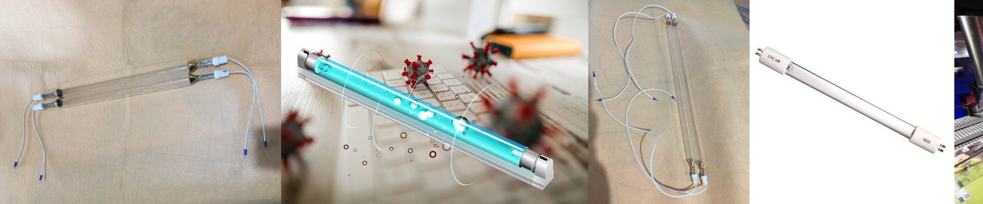
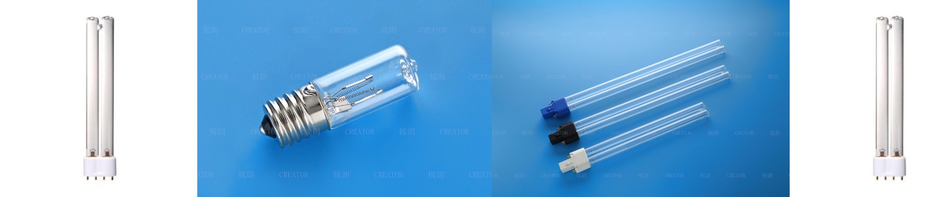
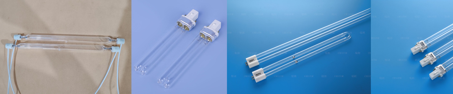
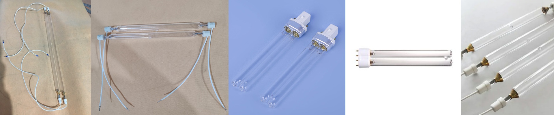
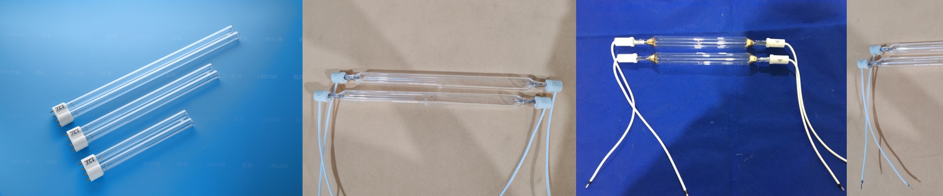
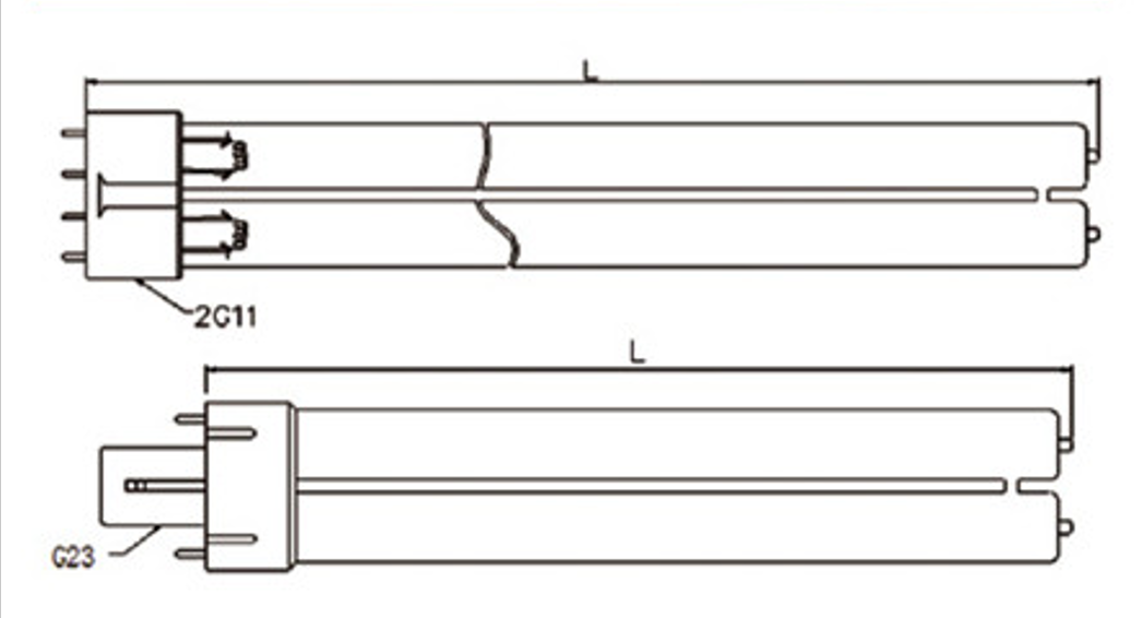
On a PCB line, micro-trace spacing leaves no room for sloppy solder mask cure. Under-crosslinked ink brings bridging, weak adhesion, and electrical failures that show up later. The outcome comes down to how well the lamp spectrum matches the photoinitiator absorption curve. What matters under the hood We build our gallium halide UV curing lamps around a tuned spectral profile, with dominant peaks at 365nm and 385nm. That narrow-band output hits the absorption bands of modern solder mask inks, driving fast photopolymerization without cooking the substrate. You get peak irradiance above 1200 mW/cm² at the arc center, measured at a 10mm working distance. The quartz body runs ozone-free, and a dichroic-coated reflector keeps spectral purity high while cutting IR load. Rated lamp life is 3000 hours, with less than 8% output decay—thanks to stable arc behavior and controlled electrode erosion. Why this works on PCBs Solder mask cure needs high energy density in micro-features, without shadowing. The 365nm/385nm combo penetrates thin ink layers while keeping definition sharp between traces, so you get complete cross-linking even in tight line/space geometries. Output stability keeps the cure window repeatable, so you hold consistent mJ/cm² run after run. These lamps run cooler than high-pressure mercury systems, which lowers the risk of board warp and lets you push line speeds higher. Power draw is down, and fewer lamp swaps mean less downtime. A few shop-floor realities These lamps are picky about position. Keep alignment and distance within ±1mm to maintain irradiance uniformity across the cure zone. Hook them into your existing UV system with matched reflectors and connectors, and double-check spectral compatibility with your ink’s photoinitiator package. For the cleanest results, pair the setup with a closed-loop radiometer to track dose and compensate as the lamp ages.